CAT6095
http://onsemi.com
2
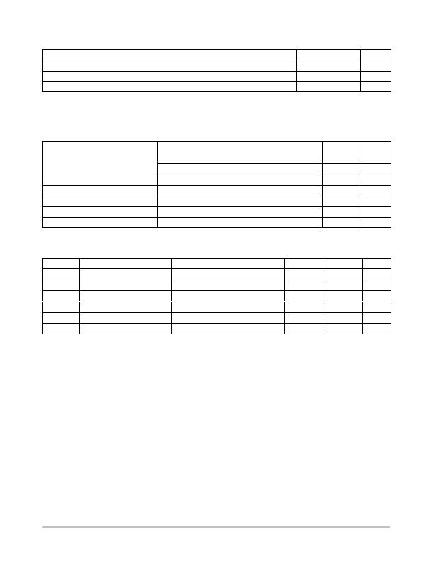
Table 1. ABSOLUTE MAXIMUM RATINGS
Parameter
Rating
Units
Operating Temperature
45 to +130
癈
Storage Temperature
65 to +150
癈
Voltage on any pin with respect to Ground (Note 1)
0.5 to +6.5
V
Stresses exceeding Maximum Ratings may damage the device. Maximum Ratings are stress ratings only. Functional operation above the
Recommended Operating Conditions is not implied. Extended exposure to stresses above the Recommended Operating Conditions may affect
device reliability.
1. The DC input voltage on any pin should not be lower than 0.5 V or higher than V
CC
+ 0.5 V. The A
0
pin can be raised to a HV level compatible
with the use of a DDR3 SPD device sharing the bus with the TS. SCL and SDA inputs can be raised to the maximum limit, irrespective of V
CC
.
Table 2. TEMPERATURE CHARACTERISTICS (V
CC
= 3.3 V ?10%, T
A
= 40癈 to +125癈, unless otherwise specified)
Parameter
Test Conditions/Comments
Max
Unit
Temperature Reading Error
Class B, JC42.4 compliant
+75癈 d T
A
d +95癈, active range
?.0
癈
+40癈 d T
A
d +125癈, monitor range
?.0
癈
20癈 d T
A
d +125癈, sensing range
?.0
癈
ADC Resolution
12
Bits
Temperature Resolution
0.0625
癈
Temperature Conversion Time
100
ms
Thermal Resistance (Note 2) q
JA
JunctiontoAmbient (Still Air)
92
癈/W
2. Power Dissipation is defined as P
J
= (T
J
T
A
)/q
JA
, where T
J
is the junction temperature and T
A
is the ambient temperature. The thermal
resistance value refers to the case of a package being used on a standard 2layer PCB.
Table 3. D.C. OPERATING CHARACTERISTICS (V
CC
= 3.3 V ?10%, T
A
= 40癈 to +125癈, unless otherwise specified)
Symbol
Parameter
Test Conditions/Comments
Min
Max
Unit
I
CC
Supply Current
TS active
200
mA
I
SHDN
TS shutdown; no bus activity
10
mA
I
L
I/O Pin Leakage Current
Pin at GND or V
CC
2
mA
V
IL
Input Low Voltage
0.5
0.3 x V
CC
V
V
IH
Input High Voltage
0.7 x V
CC
V
CC
+ 0.5
V
V
OL
Output Low Voltage
I
OL
= 3 mA, V
CC
> 2.5 V
0.4
V
发布紧急采购,3分钟左右您将得到回复。
相关PDF资料
DS1621S+
IC THERMOMETER/STAT DIG 8-SOIC
DS1624S+T&R
IC THERM/EEPROM DIG 256BYT 8SOIC
DS1626S+
IC THERMOMETER/STAT DIG 8-SOIC
DS1629S+T&R
IC THERM/RTC/CALENDAR DIG 8-SOIC
DS1631S+T&R
IC THERMOMETER DIG HI-PREC 8SOIC
DS1721U+T&R
IC THERMOMETER/STAT DIG HP 8USOP
DS1722S
IC THERMOMETER DIG 3-WIRE 8-SOIC
DS1775R7+T&R
IC THERMOM/STAT DIG 111 SOT-23-5
相关代理商/技术参数
CAT6095VP2I-GT4
功能描述:板上安装温度传感器 Dig Output Temp Sensor RoHS:否 制造商:Omron Electronics 输出类型:Digital 配置: 准确性:+/- 1.5 C, +/- 3 C 温度阈值: 数字输出 - 总线接口:2-Wire, I2C, SMBus 电源电压-最大:5.5 V 电源电压-最小:4.5 V 最大工作温度:+ 50 C 最小工作温度:0 C 关闭: 安装风格: 封装 / 箱体: 设备功能:Temperature and Humidity Sensor
CAT6201
制造商:ONSEMI 制造商全称:ON Semiconductor 功能描述:300 mA / 13 V Adjustable CMOS LDO Regulator
CAT6201VP2.GT3
制造商:ONSEMI 制造商全称:ON Semiconductor 功能描述:300 mA / 13 V Adjustable CMOS LDO Regulator
CAT6201VP2GT3
制造商:ONSEMI 制造商全称:ON Semiconductor 功能描述:300 mA / 13 V Adjustable CMOS LDO Regulator
CAT6201VP2-GT3
功能描述:低压差控制器 - LDO LDO 300 MA ADJUSTABLE
RoHS:否 制造商:Micrel 最大输入电压:5.5 V 输出电压:Adjustable 输出电流:10 mA 负载调节: 输出类型:Adjustable, Fixed 输出端数量:1 最大工作温度:+ 125 C 安装风格:SMD/SMT 封装 / 箱体:SOT-23-6
CAT6202
制造商:ONSEMI 制造商全称:ON Semiconductor 功能描述:500 mA / 13 V Adjustable CMOS LDO Regulator
CAT6202VP2.GT3
制造商:ONSEMI 制造商全称:ON Semiconductor 功能描述:500 mA / 13 V Adjustable CMOS LDO Regulator
CAT6202VP2-GT3
功能描述:IC REG LDO ADJ .5A 8TDFN RoHS:是 类别:集成电路 (IC) >> PMIC - 稳压器 - 线性 系列:* 标准包装:1 系列:- 稳压器拓扑结构:正,可调式 输出电压:1.25 V ~ 10 V 输入电压:2.9 V ~ 12 V 电压 - 压降(标准):- 稳压器数量:1 电流 - 输出:700mA 电流 - 限制(最小):- 工作温度:-40°C ~ 85°C 安装类型:表面贴装 封装/外壳:10-VFDFN 裸露焊盘 供应商设备封装:10-DFN(3x3) 包装:Digi-Reel® 其它名称:NCV8535MNADJR2GOSDKR